This course was heavily focused around independent lab work, and the last month of the course was dedicated to a final project completed in pairs. I am very thankful for having the pleasure of working with Eric Yates on the final project. He is simply one of the best computer engineers I have met at the U of G and I was very lucky to have been able to get to know him.
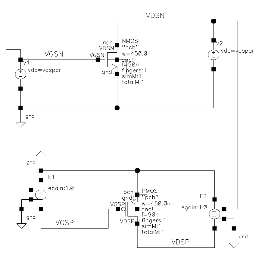
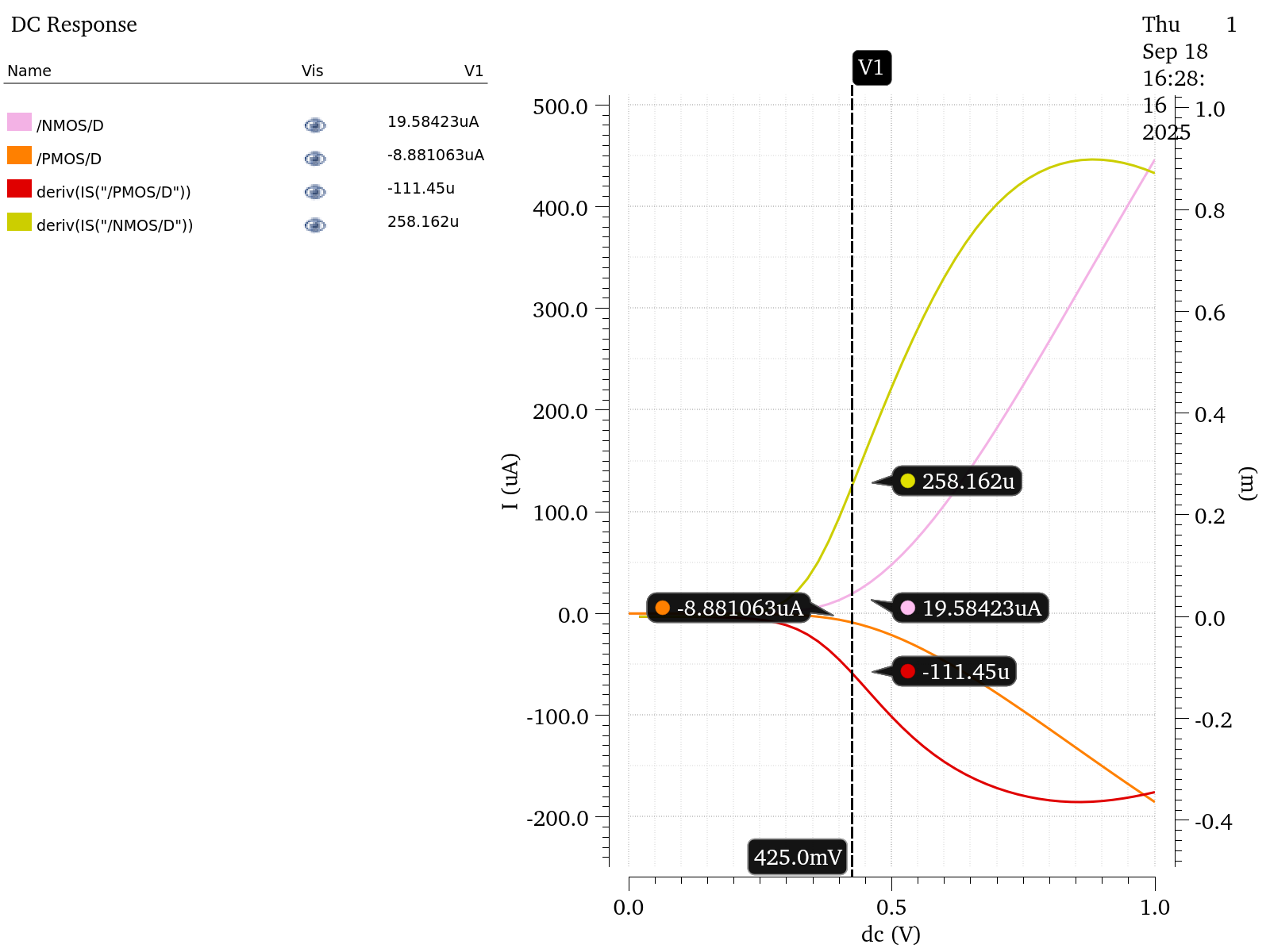
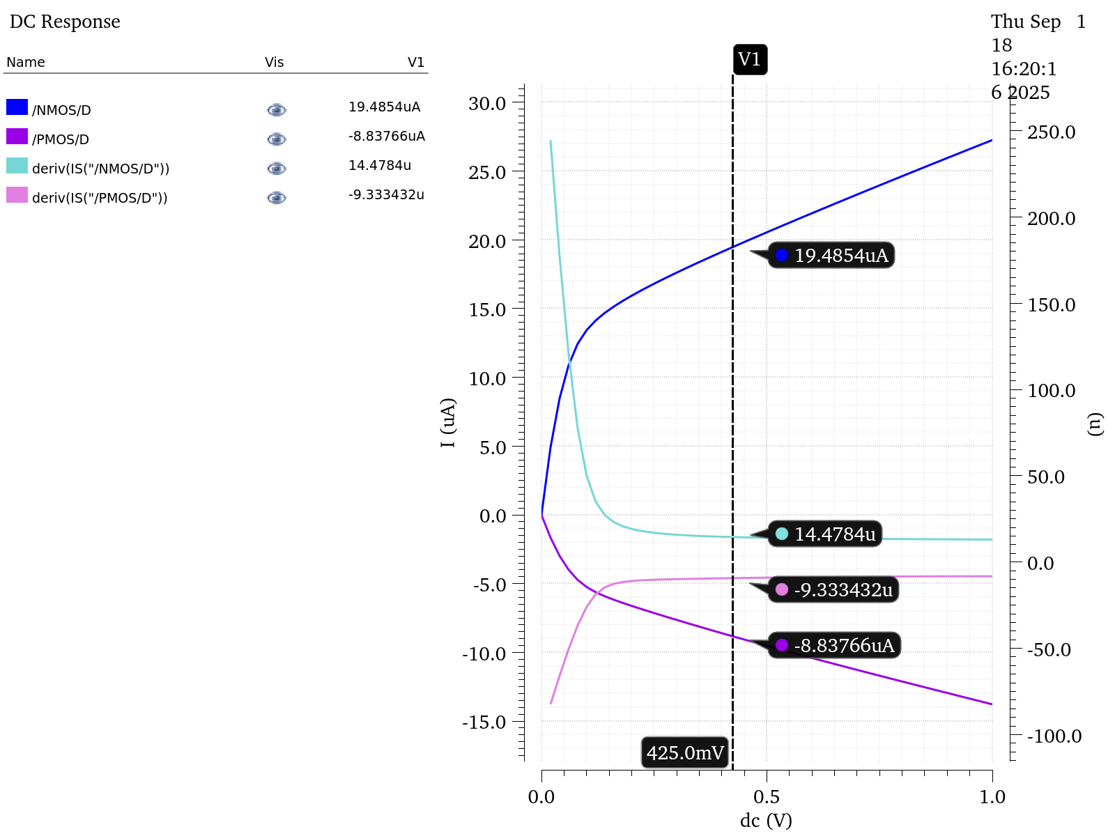
The first lab was all about Schematic entry and circuit simulation. I was dropped in head first into Cadence Virtuoso and this lab was very much a self guided exploration of the tool. Modern day electronic systems and ICs rely heavily on transistors, specifically MOSFETs using CMOS technology. MOSFETs are very versatile devices, and can be used as amplifiers, or switches. When assembled together they can make logic gates, and build large scale ICs. This lab was completed using the TSMC 65-nm CMOS technology. This laboratory was comprised of two experiments that teach the fundamentals of schematic entry and circuit simulation in Cadence Virtuoso. The first part relates to simple n-type and p-type MOSFETs. The seconds relates to a Common-source amplifier making use of the two types of MOSFETs from the first experiment. For the first part two MOSFETS were places on one schematic. They were appropriately wired up with parametric gate-source and drain-source voltages. The Schematic for the NMOS and PMOS can be seen to the right. Then a DC Simulation of the NMOS and PMOS transistors was performed. A portion of the results can be seen below. The purpose of these simulation was to characterize the MOSFETs. Some of the key values are the trans-conductance gm in microsiemens, the drain-source resistance rDS in kilo-ohms, and threshold voltage Vth in millivolts.
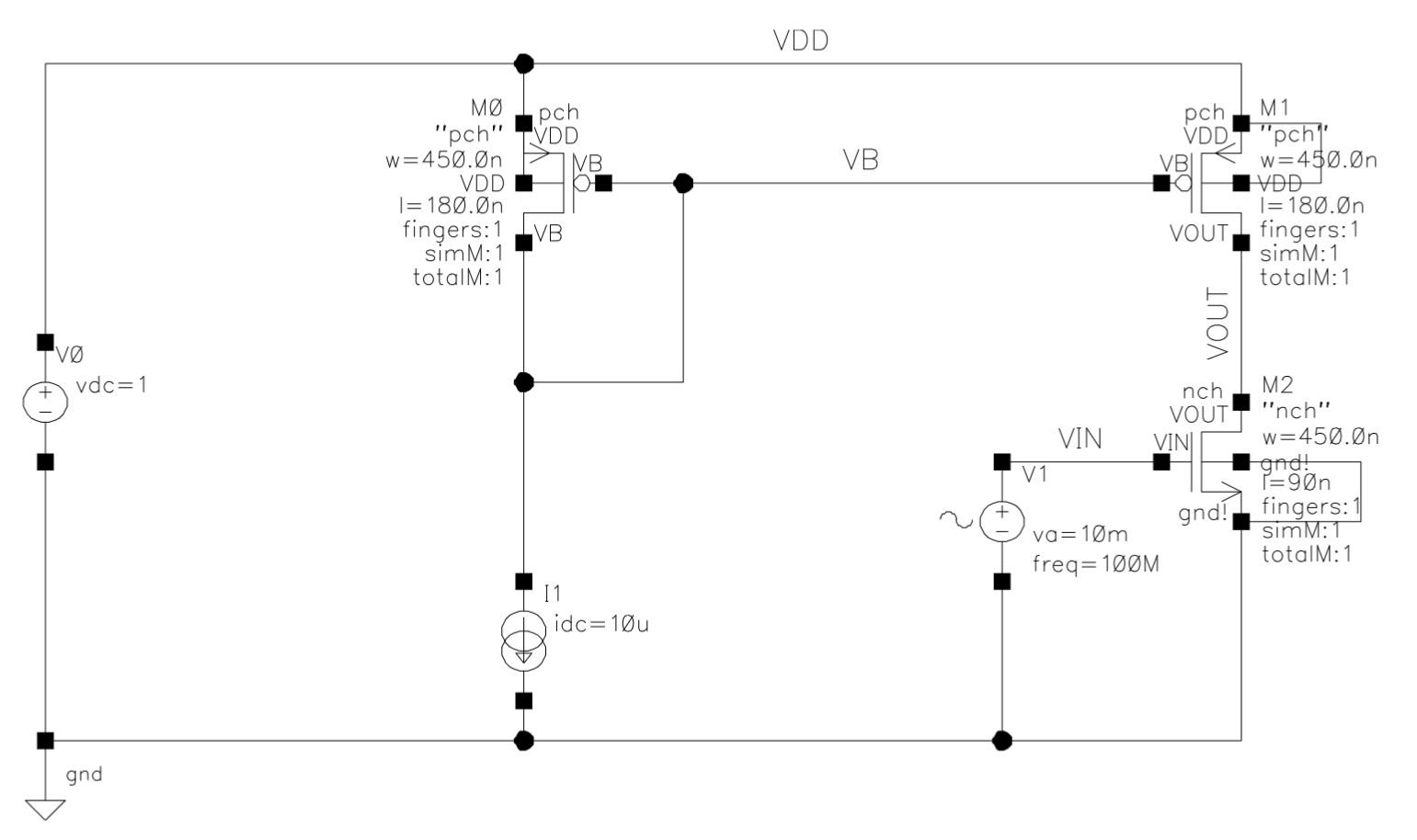
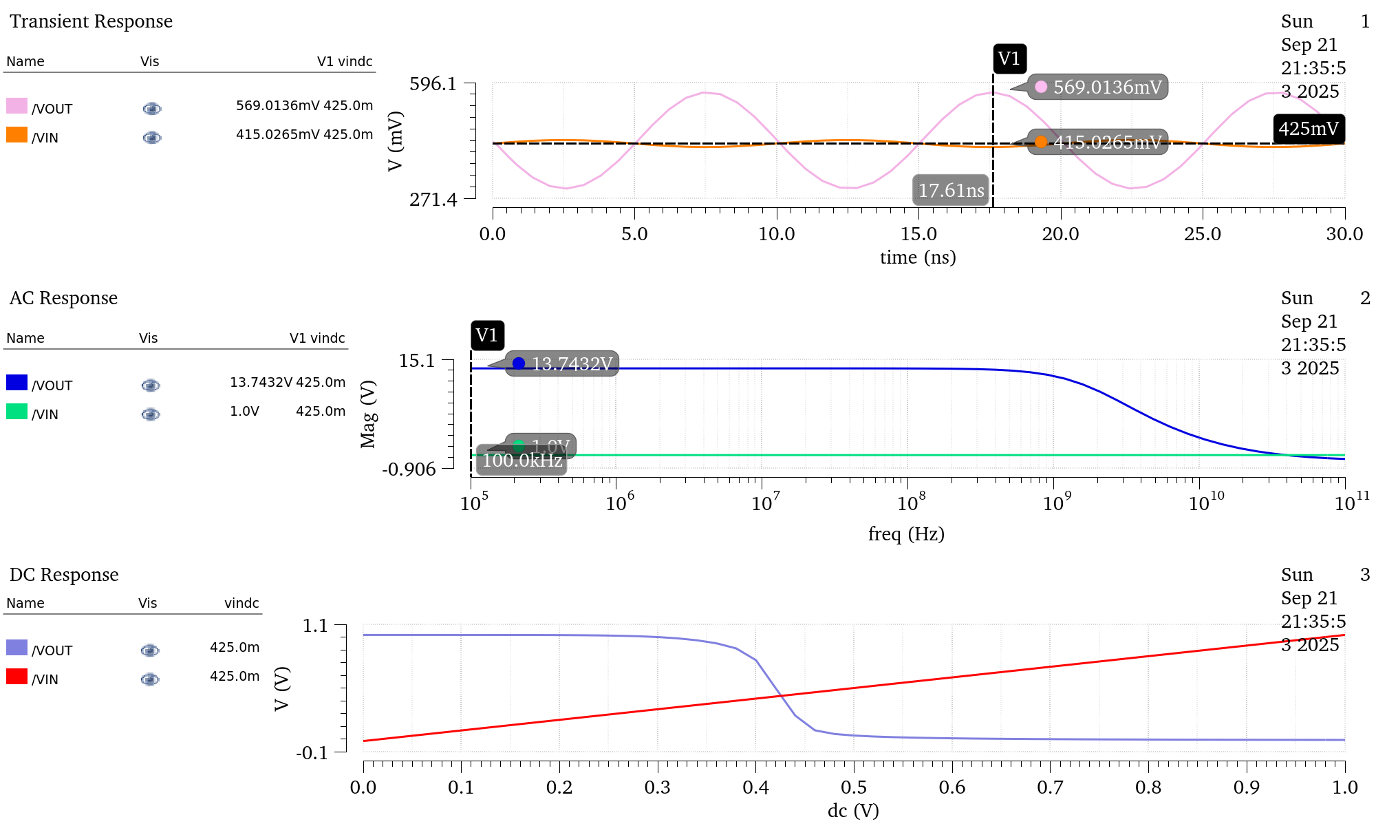
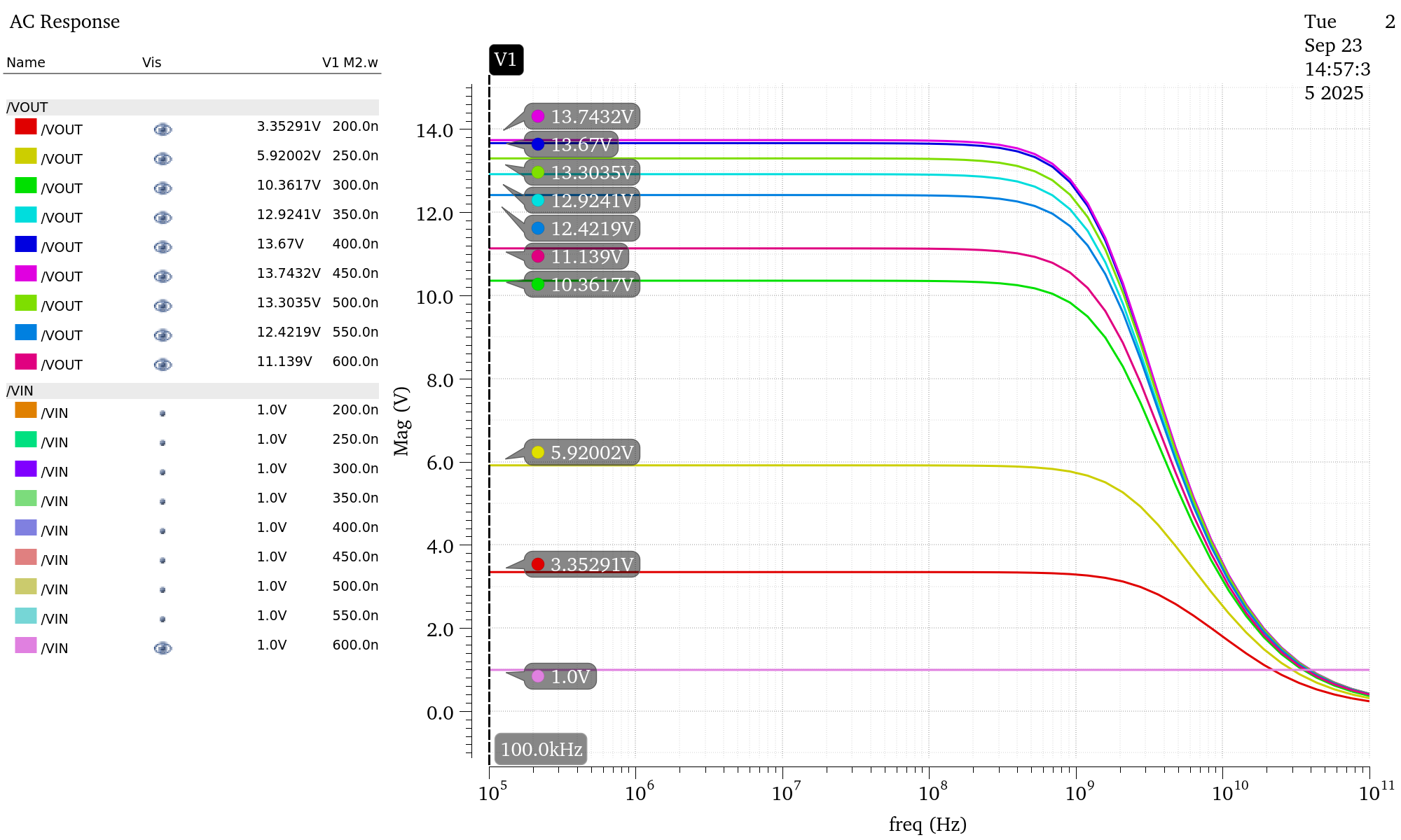
The second part of this fist lab was producing the schematic and testing a Common-source Amplifier. Using the small signal model of the CS amplifier and some of the values from the simulation in part one the gain of the amp was predicted. The calculated gain was Av = -15.09. Next the voltage gain was measured using transient and AC analysis. These simulation results can be compared with the calculated values above. A DC Simulation of the amplifier was also performed. A portion of the resulting plots from the simulation can be seen below. This simulation was at ambient temperature with no corner cases on the TSMC 65nm process. Additionally in part 2 of the experiment there was an attempt to increase the gain of the amplifier by 20%. A simulation was made this time the width of the transistor M1 was set as parameter and swept from 200nm to 600nm to see if any increases in gain could be made.
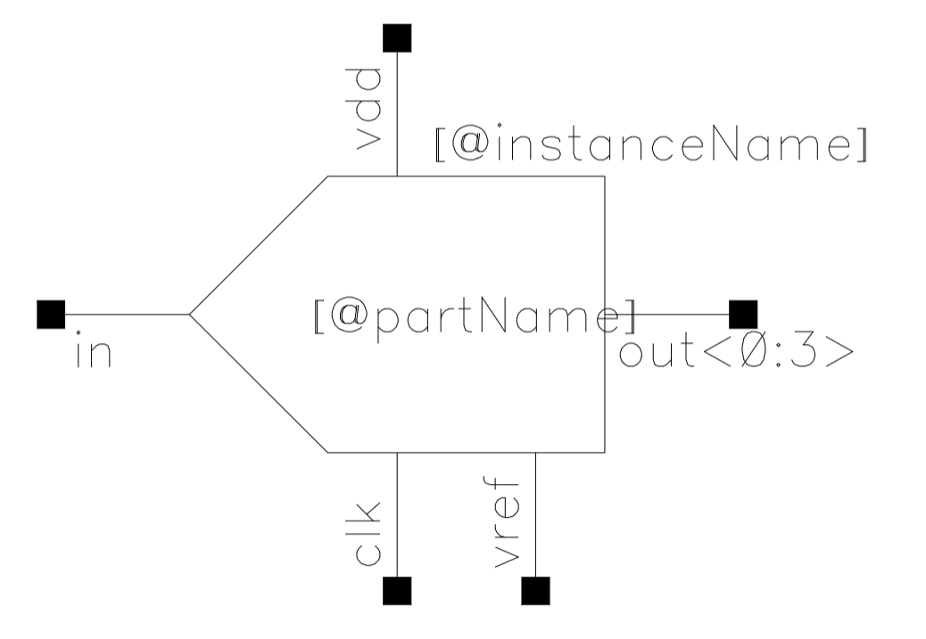
The second lab was all about Hardware descriptive languages and Verilog-A. Modern day electronic systems and ICs rely heavily on hardware descriptive languages (HDL). It would be an immense understatement to claim designing complex a IC with a million or more transistors at the schematic level as impractical. Luckily with HDLs like Verilog, and extensions that support analogue behaviour like Verilog-A this task becomes realistic. This second lab included the critical component definition and entry at the behavioural level. The end goal will was to design and implement a 4-bit DAC and ADC. The design for the 4-bit ADC was entered into Virtuoso using Verilog-A The full source code can be seen in the Full lab 2 PDF which is linked below. A symbol for the component was made which can be seen on the left. Creating this symbol for the component defined by Verilog-A lets it be used in a schematic layout too.
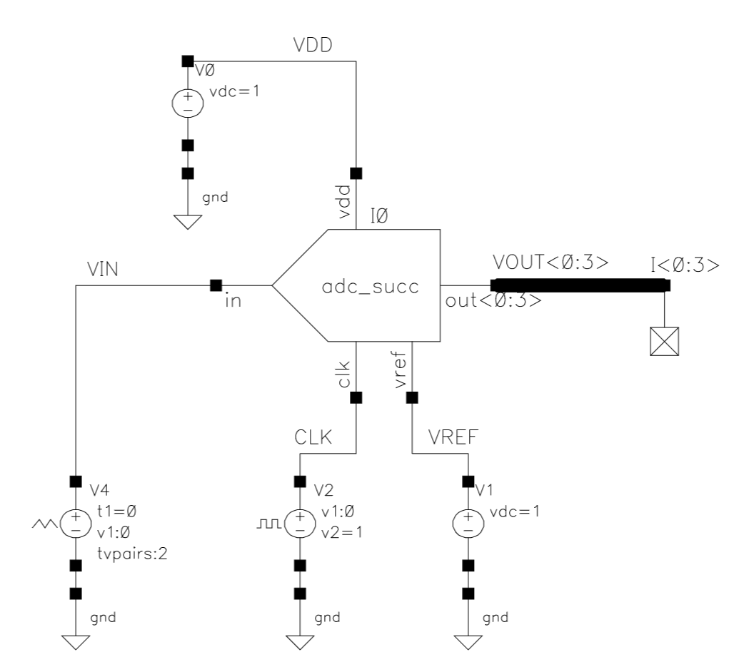
This schematic then became very helpful in setting up a test bench to validate the design of the ADC. The ADC takes a single DC voltage as an input. In the case of the test bench seen on the left the input that will be simulated is a smooth ramp input. To power the conversion the ADC also needed 1V of VDD. To scale the binary output it was given a reference of 1V. It also needed a clock pulse as input to trigger a new sample of the input voltage. The final output was a four bit value in binary. An input of 0V should give an output of 0b0000. And any input of 937.5mV or greater results in a full 0b1111.
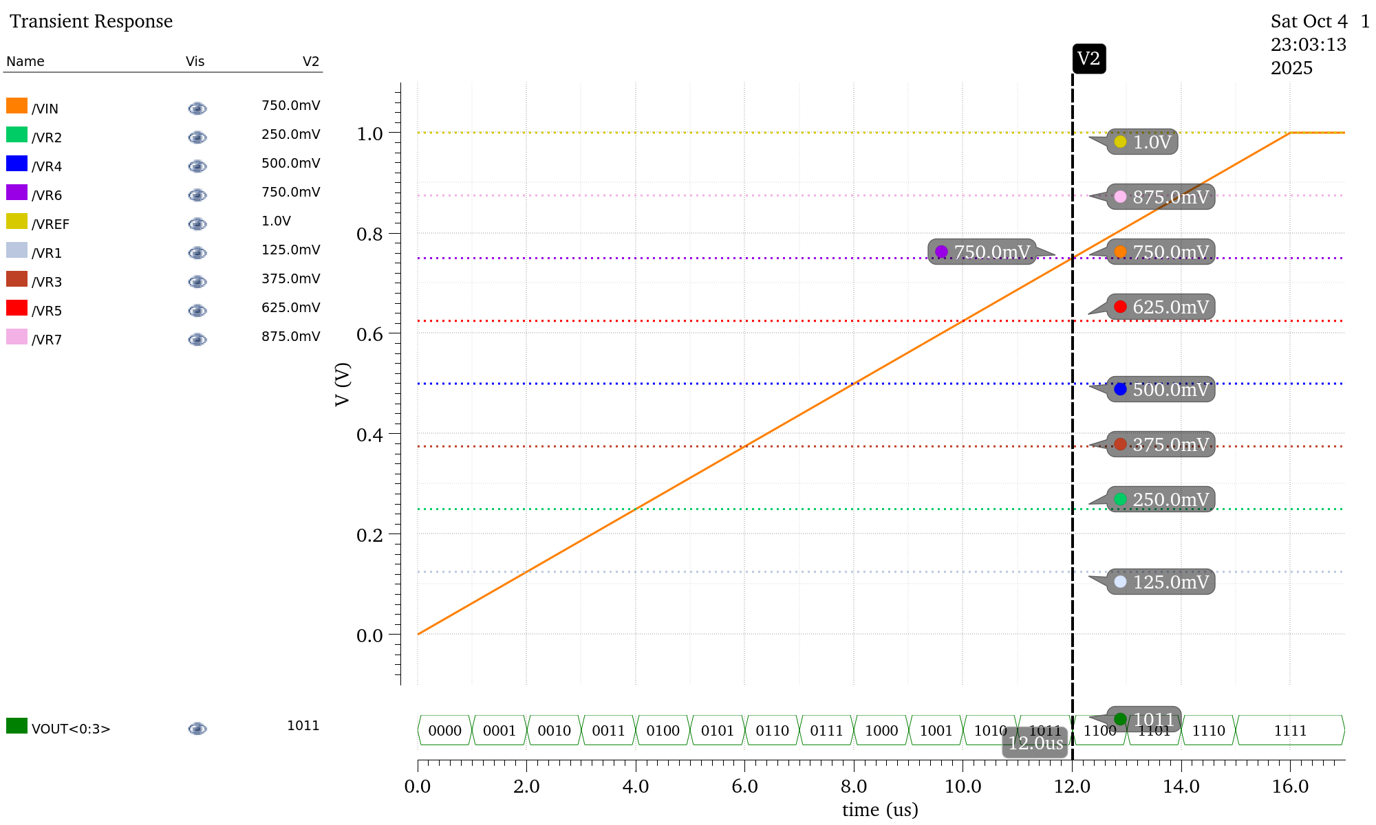
And sure enough looking at the simulation results that is exactly what was seen! This second lab also had a very similar second part that involved designing a Digital to Analog converter.
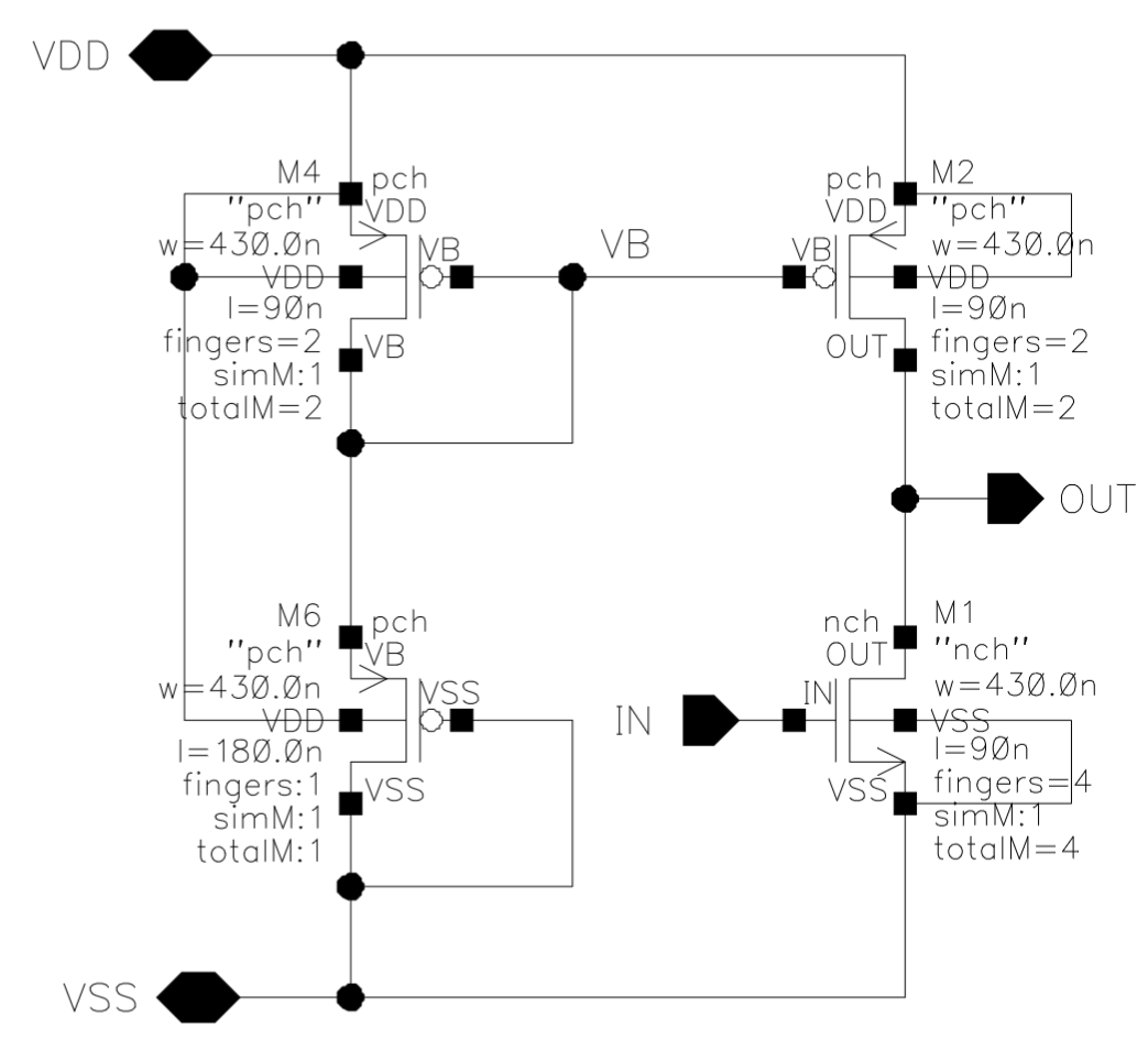
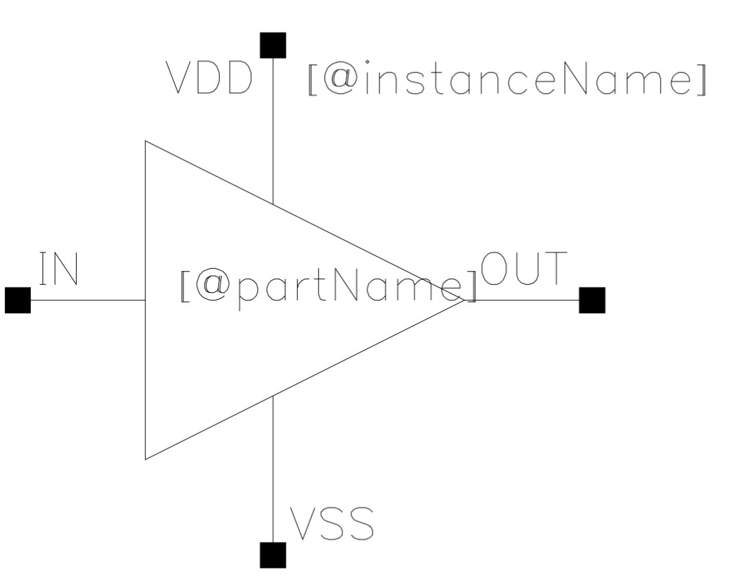
The third lab was the last one before the final project. It was all about layout drafting and verification in Virtuoso, the layout was my favourite part of the course by far! The layout process is a fundamental stage to designing any modern day electronic systems and integrated circuits. This lab explored the critical process of taking a schematic level design and translating it to a layout that can be physically realized. The end goal was to design, implement, and simulate the layout of a Common-source Amplifier. A new schematic of the CS amp was entered much like in the first lab. This CS amp was then also given a symbol. And then a test bench was created from the schematic/symbol. This was done to validate the design and to characterize when using ideal NMOS and PMOS FETs
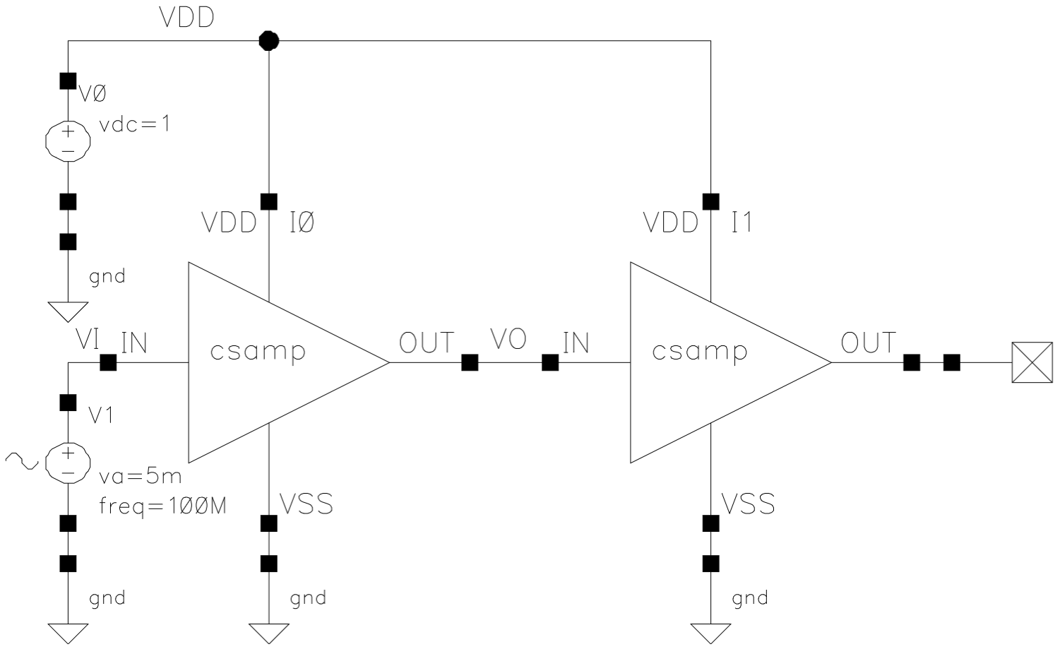
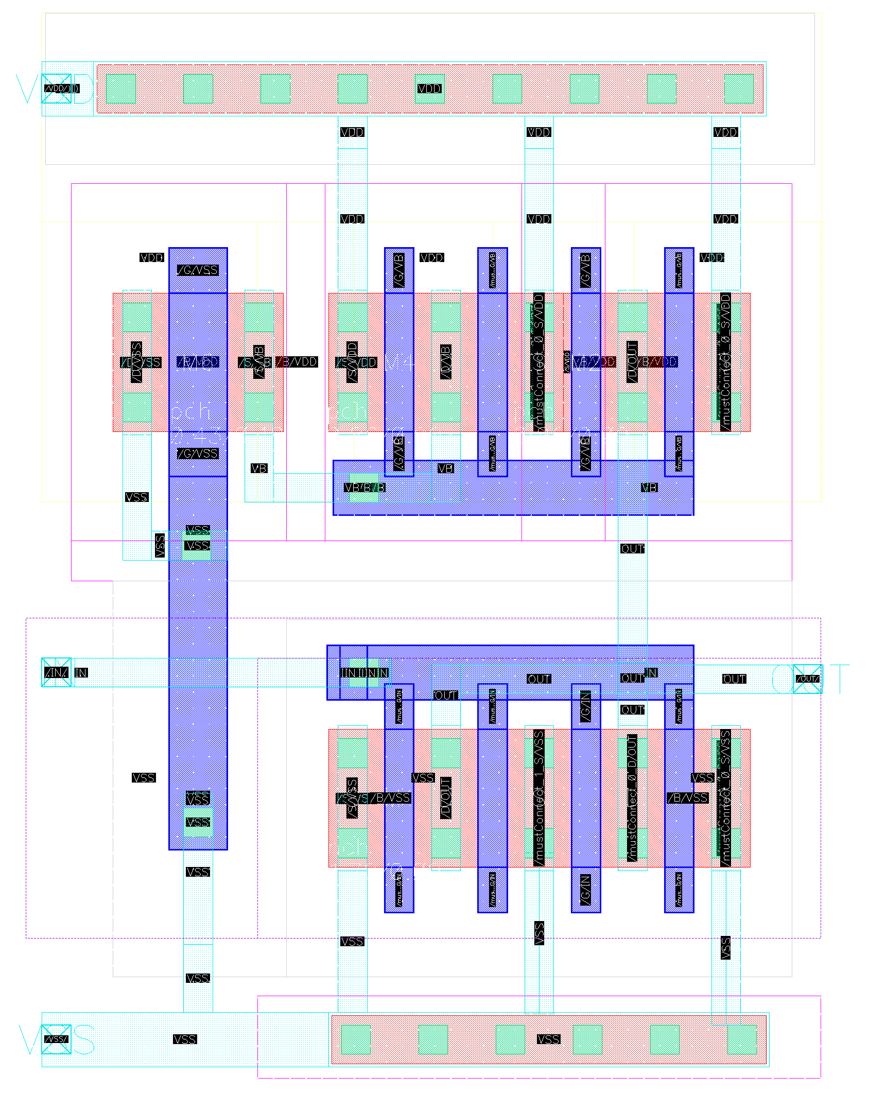
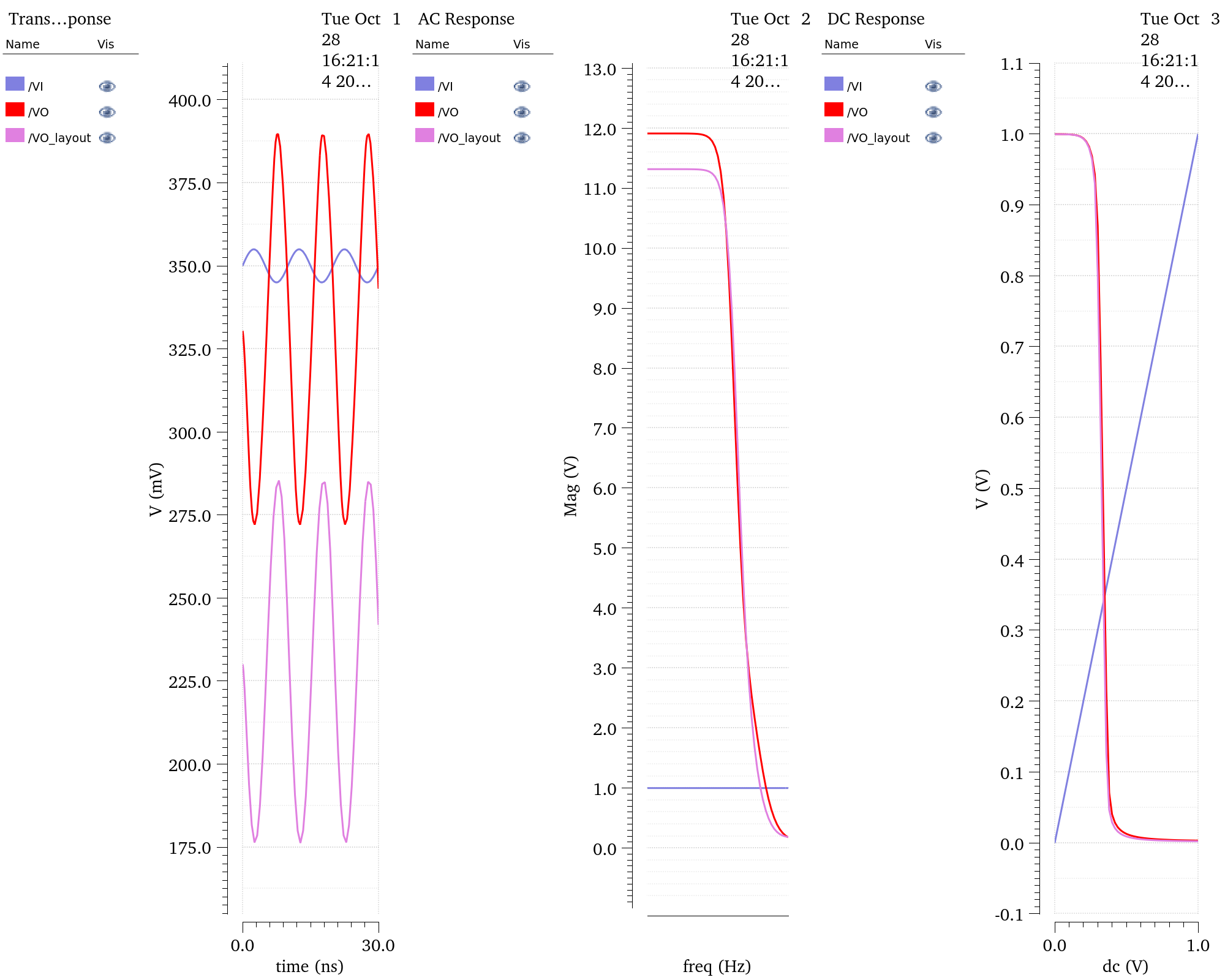
The layout was considered completed once it passed the DRC (Design Rule Check) and the LVS (Layout vs Schematic) tests. After that parasitic extraction was performed so that the layout may be simulated to account for the geometry selected. The Post-layout simulation plot was then appended to the pre-layout simulation. As seen to the right the AC and DC responses were very close but the transient response was very different.
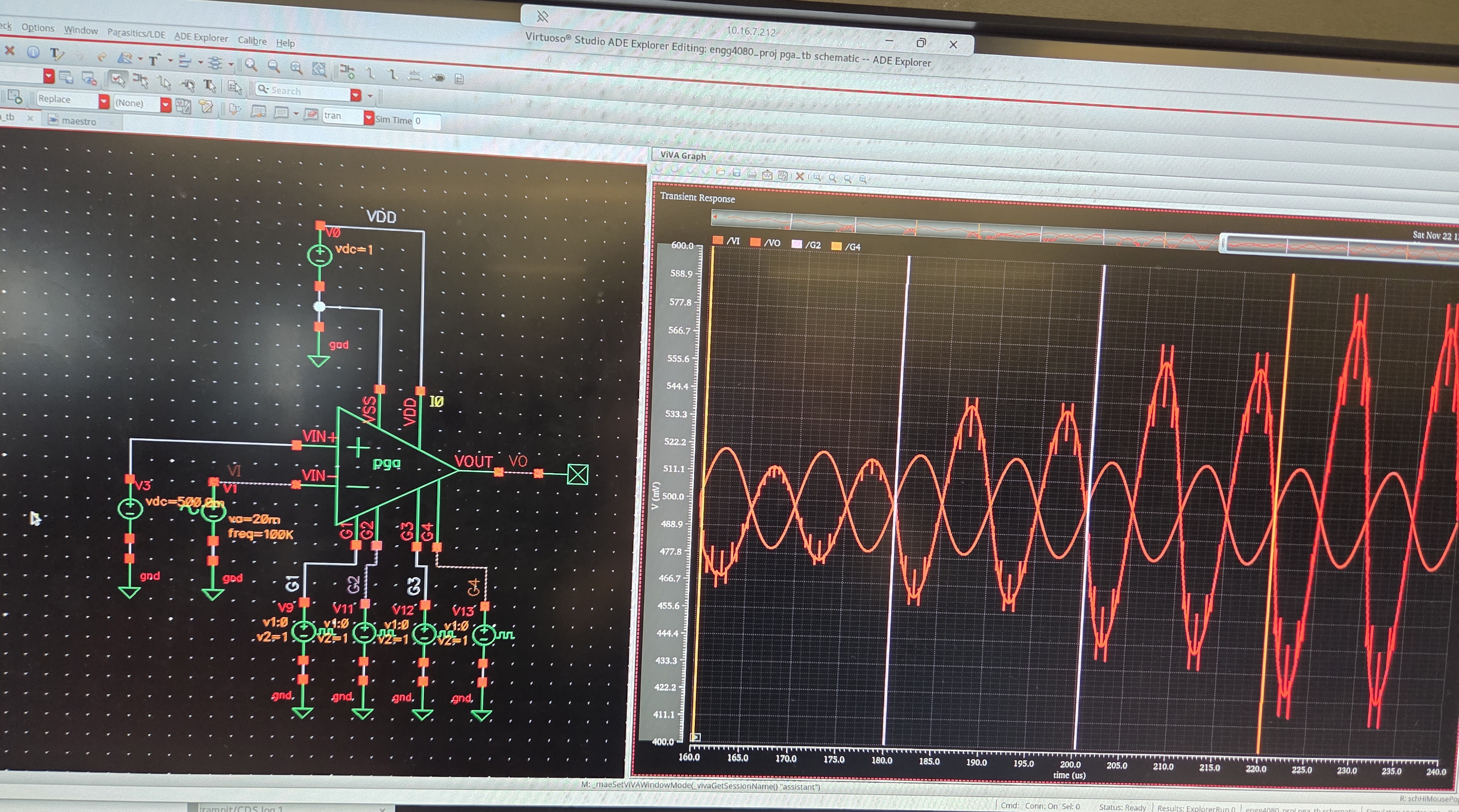
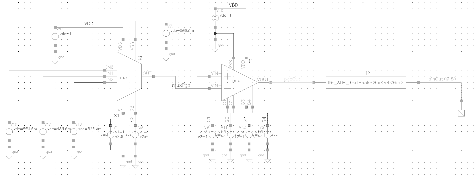
The final project was much a much more involved process than the labs. I was very lucky to have been able to work with Eric Yates for said project. The task was to fully design the analog portion of a smartwatch for the fictional company Gizmonic. The integrated circuit design for an electrocardiogram (ECG) in a smart watch application was divided into three modules: an analogue multiplexer, a programmable gain amplifier, and a 6-bit analogue to digital converter. The module designs were all to be implemented using the TSMC 65-nm CMOS technology. The watch platform has a RISC core which will provide control signals for the analogue modules. A peak into the development process for the programmable gain amplifier can be seen to the left. This was a very large project and does not lend itself well to summary. The high level top module and be seen below, and for addition details the full project PDF can be viewed.